Wednesday, May 20, 2020

How to Connect Power Switches

Power switches helps in reducing leakage power, today we will discuss about how to connect power switches as the way they are connected has direct impact on rush current & wake up time. To know more about Inrush current & wake up time please read about power switch in my previous post.
There are multiple ways we can connect enable pin of a power switch, but the best way is to mitigate the inrush current is to connect power switch cells enable pin in a daisy-chain fashion.
In Daisy chain enable pin of power switch is connected to other enable pin of power switch, which will allow  power switch to wake up in synchronous manner one after another instead of all at a time.


Power switch daisy chain fashion
Figure 1: Daisy Chain

If power switch enable in a simultaneous enable fashion, then huge rise in rush current will take place by minimising the ramp up time,.


Figure 2 : Simultaneous Enable

Referring the figure 2, we can see that at a time 4 power switch column going to power up ,suppose one column is taking I current from grid, so in simultaneous enable fashion it will take 4I from the grid at a time, which will concurrently increase our rush current.


Please refer the below link to know more about different styles of connecting enable pin of power switch

Saturday, May 9, 2020

Header Switch v/s Footer Switch

When gets to choose between one of these two switching strategy (either header or footer) area, IR drop,efficiency & design architectural issues are the key matrix.
Actually, both could be used. However, it would generate a big IR drop, which, in turn, could cause large standard cells delays.

Considering about Header switch which is being implemented by using pMOS to control VDD supply. pMOS transistors are less leaky  than nMOS transistor of same size.The disadvantage is that pMOS is having less driving capability than nMOS of a same size (mobility of electrons is higher than holes)

Considering about Footer switch which is being implemented by nMOStransistors to control VSS supply. The advantage of footer is having high drive strength & less IR . Thus, to achieve the same drive strength and IR drop, a design with footers would require less switches than a design with headers. However nMOS transistors are more leakier than pMOS & design become more sensitive to ground noise on the  virtual GND coupled through Footer switch.

Despite the obvious advantage of Footer switch ,Header Switch are generally being used in Power gating designs as in multi voltage designs demands for level shifters on signals between blocks with different supply voltages. These elements have a common ground and two power supplies. In this case, footers should not be used.

Friday, May 8, 2020

What is Power Gating Technique

Power gating is a technique to reduce Leakage power dissipation by switching off the power of blocks that are in standby mode and switching the power back on when their functionality is required.
In order to switch power off, high Vt transistors are used as switches and placed between the block PG (power and ground) pins and the PG rails.

There are 2 types of power switch

Header switchPmos transistor placed between VDD  & power rails.
Footer switch: Nmos transistor is placed between GND & power rails.

Figure 1: Header & Footer Switch


This way the controlled block, is no longer powered by the main power rails (always-on rails), but powered by a switched power rail (collapsible power).
There are multiple aspects designers need to take care of including IR drop, ramp up time, rush current, and the number of power switches added in the design. Lets discuss one by one what it is & what are there significance.

Rush Current: Current drawn by the circuit during power up known as Rush current. As when the circuit powered up all the capacitors is going to charge simultaneously at once, which fetch high amount of current from grid, cause a sudden rush of current which can damage the power switch network.
Usually we use multiple power switch in parallel to divide the power domain supply into small blocks, so by doing this the load on power switch going to reduced which helps in managing rush current

Ramp up Time: The time required for powering up a shutdown domain known as Ramp up time. It should be as less as possible.

IR Drop: To handle rush current power switches are designed to have high channel resistance which leads to high IR drop across the power switch which may cause the degrading of power in the design leads to functionality failure (as minimal supply is going to logic cells).

So, we have to design power switch which should have less IR drop by keeping in mind of Rush current which will be achieved by using two types of power switch one which is used during power up to handle rush current & the second one during normal operation

Leakage Current: As switch cell we used is of high VT  which also going to contribute in the leakage current, so we have to take care of number of power switches we used in a design.

Requirement is to minimise the ramp up time as much as possible keeping in mind of rush current.

To meet this we have different variety of power switches.Some Power switch cells have one enable control (for gating power) and some have two enable controls. The ones with two enables provide a way to control the ramp up time (power switch network) and rush current at power up. 
This is achieved by carefully designing the cell so that internally, one enable pin is connected to a smaller switch, and the other enable pin is connected to a bigger switch.(2 switches in one power switch)
To power up the switch network the smaller switch is going to turn on first to slowly bring the power supply to expected voltage level keeping rush current under control. Once the circuit gets to certain voltage levels larger switch is turned ON for normal operations of power domain logic cells while manage IR drop.

In the next post we will discuss about some power switch chain style to reduce Power Switch Rush Current. Stay Blessed :) 

Wednesday, May 6, 2020

What do you mean by Testing & Verification

Testing is a process to determine the presence of faults (not the absence of faults) in a given circuit,whereas Verification is the process to determine the correctness of a design i.e whether the design is working correctly or not.
Some other differences are as below

Testing
Verificataion
  • Testing verifies the correctness of manufactured hardware i.e gate level circuit
  • Verification verifies the correctness of a design i.e design is working perfectly or not
  •  In Testing we have a hardware on which we can apply inputs & observe the output
  • Whereas Verification works on a design which is on paper
  • Responsible for quality of a devices
  • Responsible for Quality of a design
  • Performed on every manufacture devices
  •  Performed only once prior to manufacturing

Testing can be done at below level
  • Chip level
  • Board level
  • System level
As we go down the hierarchy level the cost of testing is going to increase by 10 times,so its better to do testing in early stages of a design.
One point to be noted that no amount of a testing gives us a guaranty that a circuit is fault free,the more we test the more confidence we get about for proper working of circuit.

Sunday, May 3, 2020

Scan chain operation

Scan chain is used to find stuck at faults in the design, it involves 3 stages:
  • Shift-In
  • Capture
  • Shift-Out
In the last post we have discussed about the Scan chain, For better understanding of this post i will recommend you to visit my previous blog on Scan chain.
Lets discuss each stage one by one

Shift-IN
Let us consider the circuit shown in figure 1 to demonstrate how the scan chain functions,having 7 primary inputs (including clk & Scan_enable), assuming output of AND gate SA-0
  • When SE = 0, it will act in normal mode & Scan flops will  get the input from the D pin of mux which has connected to the logic cone.
  • When SE = 1, flops will get input from T1 pin of mux, the output of one flop is connected to next input of flop acting as a shift register.
As we can see that we don’t have direct controlability on the input pins of faulty gate, we have to use scan chain to pass the test vectors to it.
                                   Inputs of faulty AND gate =  QFF1 + QFF3

Example of how scan chain find the faulty gate in the circuit or design
Figure 1

By enabling Scan enable (SE =1) if we pass “101” (test vectors) through Scan_in  & shift a pattern using clk , then at the 3rd clock pulse we will get “11” inputs of faulty gate.See below table

CLk
FF1
FF2
FF3
0
X
X
x
1
1
X
X
2
0
1
X
3
1
0
1

This whole Scan_in cycle phase is known as Shift in.

Capture
This is the second phase in the scan mode operation known as Capture. After the successfully shifting of test vectors in the design we have to capture the output of faulty AND gate.
For this we have to do:
·    Disable the Scan_enable( SE =0)
When SE = 0, flops will act in normal mode ,so during this period the “d” input of the flop gets its input from the output of  combinational logic,i.e FF2  input gets from the output of faulty gate.
·    Apply one clock pulse to latch data QFF2
Applied one clock pulse which will latch the FF2 flop data, which we are trying to observe.

Shift-Out
This is the 3rd phase of scan mode operation in which we will observe the output of FF2. As QFF2  is internal to design, we have to enable Scan mode again (SE = 0) which helps in shifting data bit by bit with clk  until it pops out from scan_out.
The number of clock pulses that are to be applied for shifting the value depends on how deep the capturing flop lies in the circuit. Output from scan_out is compared with the expected value , if its not match we can conclude that there is some problem with the element that drives it, i.e if  logic 0 pops out from scan_out we can conclude that Gate is SA-0. Figure 2 shows the sequence of events that take place during scan-shifting & scan-capture.

explaining the 3 modes of scan chain scan_in , capture, scan_out
 Figure 2: Waveform

The same cycle repeat for each and every node where fault can occur.As testing contribute more than 50% cost of chip in which testing time plays a crucial role, so to reduce test time we have to increase the shift frequency but there is a trade off with power dissipation.
During scan mode toggling of flops & combinational logic block will be there which are a part of large scan chain leads to dynamic power dissipation & temperature hotspots around that region which can create some new violating paths.
So testing is done only in low frequency mode by taking care of test time & power dissipation in mind.

Please let me know if you any doubts in this specific post. In the next post we will discuss about the Scan chain length & reordering concept. Stay Blessed :)

Saturday, May 2, 2020

What is Scan Chain

Scan chain is a testing  method to detect various manufacturing faults in the silicon. Although many types of manufacturing faults may exist in the silicon,these could be the result of poor processing (process variation) which leads to shorts and opens.These shorts and opens in the transistors known as stuck-at-one (ST-1) or stuck-at-zero (ST-0) faults.
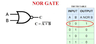
For e.g : Let's consider the 2-input NOR gate, showing below both logical & physical equivalence.
If  output pin of NOR gate (z) is Stuck at 0, how its physical defect look like


explaining stuck at fault in logical & physical representation
Figure 1: Stuck at 0 fault

From Figure 1 we can see that a short circuit path (low resistance path) has been created between the VCC & GND, which makes the output always 0 whatever be the inputs at gate terminal.

How to detect Stuck at fault
Now, how we will identify faults,Taking the above example of  2 input NOR gate, whose output pin (z) is ST-0,all we need to apply a set of input signals which makes the output of NOR gate high, if there is no fault then the output will be high for set of inputs "00" otherwise we can conclude that the gate is faulty!


Figure 2: NOR gate
we don't have to check every input or output for faults, this we can reduce to a lot with fault equivalence & dominance technique that we will discuss later.
So, using Scan we can control the inputs of gates which are inside the chip & observe the output & we determine whether the gate is faulty or not.

Scan Flip Flop
Scan Flip flop is like normal flop but having a difference of  by the fact that multiplexer has been added at the D pin of flip flop,


Figure 3: Scan flip flop

Multiplexer has 2 inputs & 1 Select line, For normal mode TE(Test Enable) of Scan flop will be 0
& it will work as normal flop, for Test mode mode TE = 1 , test vectors will be applied through TI (Test Input ) pin in the design with the help of Automatic test pattern generator.
In Scan mode (test mode) all the flops have been hooked up to form giant shift register , in which output of one flop Q has been connected to the input D pin of next flop,forming a chain of scan registers (Scan chain) which makes easy to check any stuck at fault in the design, but have to take care of chain length & frequency that we will discussed in next post.
  • Scan_in: Scan_in is the pin name which is connected to the input of the first scan flop in the scan chain to pass the test vectors (series of 1's or 0's)
  • Scan_out : The output pin through which shifted pattern comes out.
  • Scan_enable : Through which we can enable or disable the Scan mode.
In the next post we will discuss about how Scan chain functions. Please let me know if you have any queries in this post.Stay Blessed :)